The 9th Asia-Pacific Workshop on Widegap Semiconductors (APWS2019) was held in Okinawa, Japan from November 10 to 15, 2019. Researchers, scientists, and entrepreneurs from the Asia and Pacific region joined those from other parts of the world in stimulating discussions on widegap semiconductors. APWS2019 focused on the science and technology of widegap semiconductors, including III-nitrides, silicon carbide, oxides, diamond, and other materials. Research has led to developments in optical and electronic devices, including those for environmental and energy applications. Nobel laureate Prof. Hiroshi Amano of Nagoya University in Japan gave a plenary talk titled “Wide-bandgap semiconductors as key materials in realizing zero emission of greenhouse gases”. In his presentation, he discussed vertical GaN power devices as an important technology for all-GaN electric vehicles and the internet of energy.
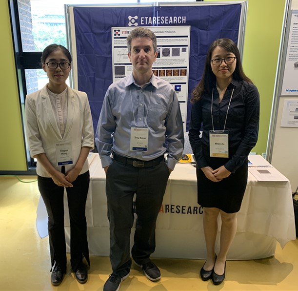
Led by its CEO Dr. Baker, Eta Research participated in the vendor exhibition and brought some samples of their GaN wafers. The company displayed two pieces of 5 inch as-grown GaN wafers and three pieces of 4 inch final GaN wafers after the polishing process. A lot of visitors dropped by the booth and they were impressed by the achievements that were made by the company. Relevant technical experts, professors, and researchers also had detailed discussions with Dr. Baker about GaN wafers and their applications. Eta believes that as more customers get to know the company and the high quality GaN wafers, new and improved GaN on GaN devices will be developed. Eta is ready to ship GaN wafers around the whole world.


