Eta Research, a Chinese semiconductor company with headquarters in the new Lingang Free Trade Zone of Shanghai, announces that they are now selling n-type 100 mm GaN wafers with an epitaxial ready polish.
Eta Research uses the HVPE method to produce GaN wafers. The company has completed the R&D necessary for commercialization of GaN wafers resulting in their unique HVPE equipment, wafer separation process, and polishing process. In 2018, the company demonstrated as-grown GaN wafers of 100 mm diameter which can be cut to 2” and 3” wafers as the finished size. In 2019, the company has developed nearly 5” as-grown GaN wafers which can be cut and processed into 100 mm wafers.
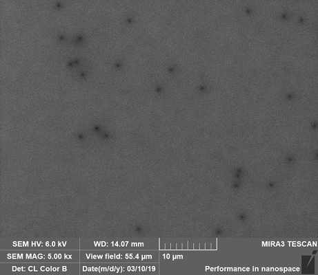
The company puts a strong emphasis on the importance of the crystal quality and lattice curvature. The typical rocking curve FWHMs of the as-grown wafers are 50 to 60 arcsec for both the (002) and (102) reflections. The threading dislocation density has been measured as 1E6 /cm2 based on CL of polished wafers. The lattice curvature is important as a measure of the offcut variation across the wafer. The center point offcut is specified at 0.35° toward the GaN m-direction and that can be modified according to the customer’s requirement. The lattice curvature radius is greater than 10 m, with the target around 30 m or larger.
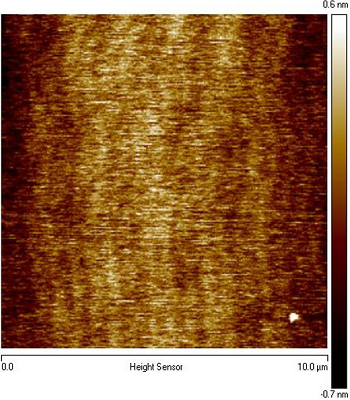
The company has developed their own polishing process for GaN, resulting in AFM average roughness over 10 um images of < 0.3 nm. They have grown MOCVD GaN epi-layers and device structures on the GaN wafers. The MOCVD-grown layers show good surface morphology and have XRD rocking curve FWHMs similar to that of the substrate.
Currently, small quantities of 100 mm GaN wafers are for sale, as well as 2” and 3” wafers. At the end of 2019, more HVPE capacity will be brought online in the new production factory located in Tongling, Anhui Province, China. The company anticipates the ability to supply high volume customers in the near future. Furthermore, working with their epitaxial growth partners, Eta Research can offer GaN wafers with MOCVD epitaxial layers for interested customers.
For additional information, see www.etaresearch.com. Email inquiries can be sent to info@etaresearch.com.


