The International Workshop on Nitride Semiconductors 2018 (IWN 2018) was held from Nov.11th to 16th, 2018 at Kanazawa, Japan. The workshop is held every two years and it gathers together scientists, experts, researchers, entrepreneurs, professors, and students to discuss nitride-related materials, such as GaN, AlN, and InN. Professor Hiroshi Amano, Nobel Prize winner in Physics of 2014, delivered a keynote speech and declared the commencement of IWN 2018.
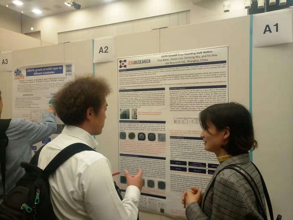
Eta Research presented a technical poster and an exhibition booth at the workshop to promote our free-standing GaN wafers. Moreover, we took some samples with us to attend the exhibition, such as 4 inch as-grown GaN wafers, 2 and 3 inch polished free-standing GaN wafers, which caught the eyes of many experts and potential customers. Some professors from universities and institutes were impressed when they learned that Eta was founded only 3 years ago and achieved so great results already. They were excited to know that a domestic Chinese company is planning to do mass production of large size of GaN wafers soon. A lot of our potential customers visited our booth and talked with our technical representatives to learn more about the GaN wafers. Some of them even asked us to deliver quotes immediately since they were very interested in our wafers.
Meanwhile, our technical poster also attracted attention from scientists and experts from different countries. They had further professional discussion with our technical engineers about some details of GaN wafers. After talking with some potential customers, we are more confident to promote our GaN wafers widely in the near future.


